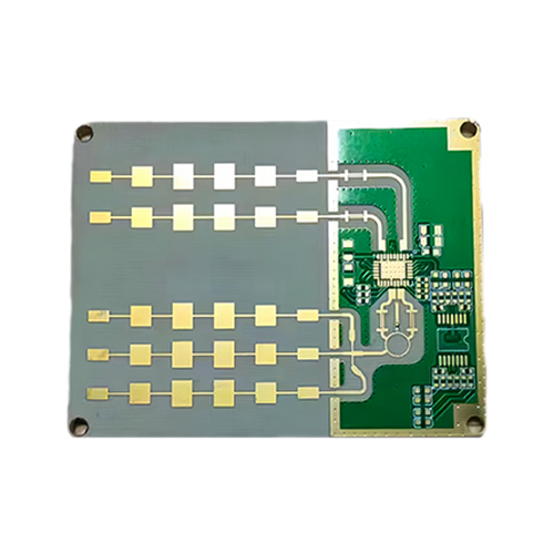
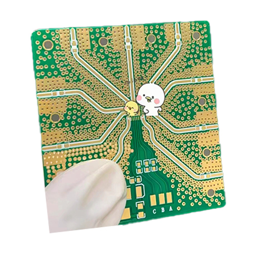
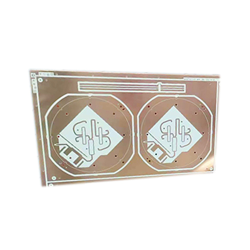
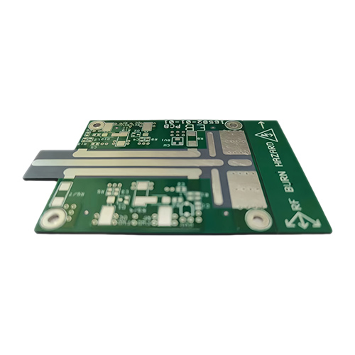
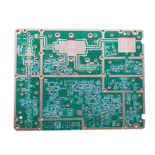
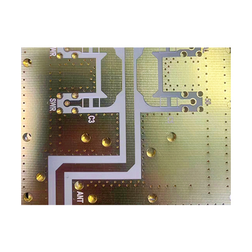
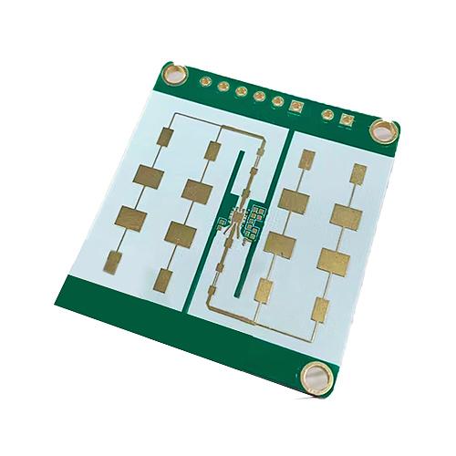
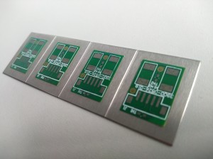
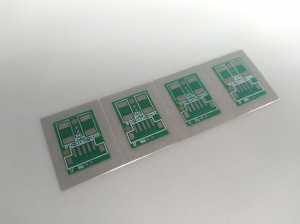
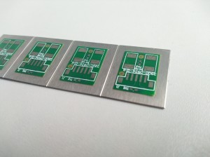
- 4 Layer RO4003C+RO5880 PCB Board
- 【Brief】:
*ROGERS and ISOLA material high-frequency PCB circuit board PCB RO3006, 4003435, 0453, 3588, 0600, 2601
*High-frequency plate processing instructions:
1. Our commonly used high-frequency plate supply are: ROGERS Rogers, TACONIC series, high-frequency microwave PTFE circuit board, Teflon Teflon, polytetrafluoroethylene circuit board
2. The commonly used inventory is Rogers 4000 series: RO4350B/RO4003C Thickness: 0.254 0.508 0.762
3. If we have no inventory, we need to confirm the delivery time to the plate supplier. If the supplier has inventory, the delivery time should be 1-5 days.
4. All high-frequency plates can be mixed with FR4 plates and PP, and Rogers 4000 series can synthesize FR4 mixed plates with RO4350BPP.
- 【Series】:Rogers PCB
Pls see our Sepecial Roger PCB board below:
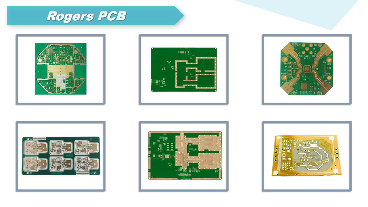
PCB Capability
| Rogers PCB Capability | |
| Materials |
RO4003C, RO4350B, RO4360, RO4533, RO4535, RO4730, RO4232, RO4233, RO3003, RO3006,
RO3010, RO3035, RO3203, RO3206, RO3210, RO3730, RO5780, RO5880, RO6002, RO3202, RO6006
|
| Maximum Lager Count | 20 Layers |
| Maximum Panel Size | 17″ x 23″ (432 x 584 mm2) |
| Min. Board Thickness | 1.0mm Al, 4 mils (0.1 mm) FR4 |
| Copper Clad (inner) | 1/2 oz, 1 oz, 2 oz, 3 oz, 4oz |
| Copper Clad (outer) | 1/2 oz, 1 oz, 2 oz, 3 oz, 4 oz |
| Surface Finishes | ENTEK 106A, Immersion Gold, HAL, immersion silver |
| Solder Mask | LPI: Taiyo PSR 4000, Tamura DS2200, Probimer 77MA |
| Minimum Trace (width) | 12.0 mils (0.30 mm) |
| Minimum Trace (spacing) | 12.0 mils (0.30 mm) |
| Minimum PAD-TO-PAD TOL. | ± 3 mils (± 0.76 mm) |
| Hole Size Tolerance (NPTH) | ± 2 mils (± 0.05 mm) |
| Hole Size Tolerance (PTH) | ± 3 mils (± 0.076 mm) |
| Minimum Hole Size | 20 mils (0.50 mm) |
| Outline Dimensional Tol. | < ± 10 mils (0.25 mm) |
| Ionic Cleanliness | < 5 mg/in2 of NaCl (0.775 mg/cm2) |
| Impedance Control | ± 10% (Differential) |
| Warpage |
< 1% |
PCB advantages:
1 R&D team support
2 UL, RoHS,ISO9001,SGS
3.IPC class2
4.Advanced production line and promtly delivery.
5,Honest Credibility in China.
6.Professional and abundant experience in PCB.
7.Competitive price and good quality.
8. Excellent after-sales service.
Trade Terms:
1. We have no MOQ.
2. Payment Term:T/T or Western Union.
3. Delivery ways:UPS,FEDEX,DHL etc,door to door service by sea or air etc.
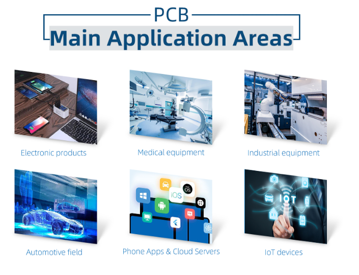
Application:
Our Service:
1.Reply your enquiry in 2 working hours.
2.Experienced staffs answer all your questions in fluent English.
3.Customized design is avaliable OEM&ODM are welcomed.
4. Exclusive and unique solution can be provide to our customer by our well-trained and professional engineers and staffs.
5. Special discount and protection of sales area provided to our distributor.
| PCB Prototype Lead Time: | ||
| Item | General time | Quick Turn |
| 1-2 | 4 days | 1 days |
| 4-6 Layers | 6 days | 2 days |
| 8-10 Layers | 8 days | 3 days |
| 12-16 Layers | 12 days | 4days |
| 18-20 Layers | 14 days | 5 days |
| 22-26 Layers | 16 days | 6 days |
| Note: Base on all data received by us and must be complete and problem free, Lead time is ready to ship time. | ||
FAQ
Q1: Are you a factory or trade company?
A1: We have our own PCB manufacturing & Assembly factory.
Q2: What’s your minimum order quantity?
A2: Our MOQ is not the same based on different items. Small orders are also welcome.
Q3: what file we should offer?
A3: PCB:Gerber file is better,( Protel,power pcb,PADs file), PCBA : Gerber file and BOM list.
Q4: No PCB file/GBR file, only have the PCB sample, can you produce it for me?
A4: Yes, we could help you to clone the PCB. Just send the sample PCB to us, we could clone the PCB design and work out it.
Q5: What any other information should be offered except for file?
A5:Following specifications are needed for quotation:
a) Bese material ; b) Board thickness ; c) Copper thickness ; d) Surface treatment; e) Color of soldermask and silkscreen; f) Quantity


