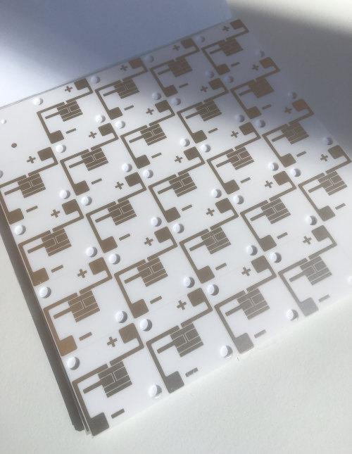
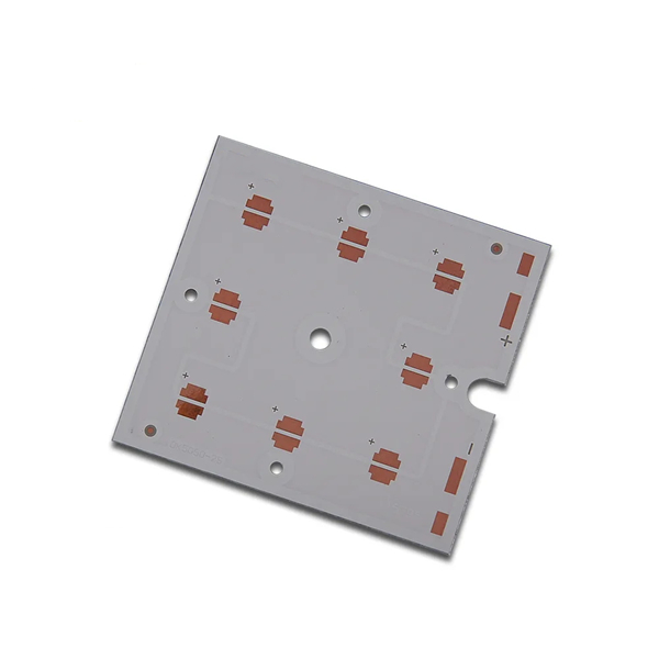
- LED Light Ceramic Circuit board
- 【Brief】:
Ceramic substrate pcb Ceramic substrate refers to the copper foil directly bonded to
the alumina (Al2O3) or aluminum nitride (AlN) ceramic substrate surface (single or double) at high temperatures
on a special process board. The prepared ultrathin composite substrate has excellent electrical insulation performance.
- 【Series】:Ceramics(Metal core PCB )
1.Introduction of LED Main Mother Aluminum PCB
Landes Circuits is capable of providing full turnkey and partial turnkey printed circuit board assembly services. For full turnkey, we take care of the entire process, including preparation of Printed Circuit Boards, procurement of components, online order tracking, continuous monitoring of quality and final assembly. Whereas for partial turnkey, the customer can provide the PCBs and certain components, and the remaining parts will be handled by us.
Features-Our Products Advantage
1. Over 10 years experience manufacturer in PCB Assemble and PCB field.
2. Big scale of producing makes sure that your purchase cost is lower.
3. Advanced production line guarantees stable quality and long life span.
4. Produce almost any PCB as your requirement.
5. 100% test for all customized PCB products.
6. One-stop Service ,we can help to purchase the components.
Metal Core PCB Capability
| Ceramic PCB Capability | |
| Materials | Aluminum ,copper,Ceramic |
| Maximum Lager Count | 4 Layers |
| Maximum Panel Size | 17″ x 23″ (432 x 584 mm2) |
| Min. Board Thickness | 1.0mm Al, 4 mils (0.1 mm) FR4 |
| Copper Clad (inner) | 1/2 oz, 1 oz, 2 oz, 3 oz, 4oz |
| Copper Clad (outer) | 1/2 oz, 1 oz, 2 oz, 3 oz, 4 oz |
| Surface Finishes | ENTEK 106A, Immersion Gold, HAL, immersion silver |
| Solder Mask | LPI: Taiyo PSR 4000, Tamura DS2200, Probimer 77MA |
| Minimum Trace (width) | 12.0 mils (0.30 mm) |
| Minimum Trace (spacing) | 12.0 mils (0.30 mm) |
| Minimum PAD-TO-PAD TOL. | ± 3 mils (± 0.76 mm) |
| Hole Size Tolerance (NPTH) | ± 2 mils (± 0.05 mm) |
| Hole Size Tolerance (PTH) | ± 3 mils (± 0.076 mm) |
| Minimum Hole Size | 20 mils (0.50 mm) |
| Outline Dimensional Tol. | < ± 10 mils (0.25 mm) |
| Ionic Cleanliness | < 5 mg/in2 of NaCl (0.775 mg/cm2) |
| Impedance Control | ± 10% (Differential) |
| Warpage | < 1% |
| PCB Prototype Lead Time: | ||
|
item |
General time |
Quick Turn |
|
1-2 Layers |
4 days |
1 days |
|
4-6 Layers |
6 days |
2 days |
|
8-10 Layers |
8 days |
3 days |
|
12-16 Layers |
12 days |
4 days |
|
18-20 Layers |
14 days |
5 days |
|
22-26 Layers |
16 days |
6 days |
| Note:Base on all data received by us and must be complete and problem free, Lead time is ready to ship. | ||


